

High-Speed Test Access for Chiplets, CPC, and CPO: Die, Substrate, and Package-Level Solutions
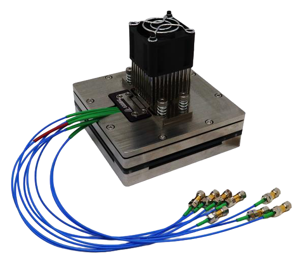
Attendees of this webinar will learn how high-density, solderless electrical access supports characterization of processors, switches, and custom ASICs at die, substrate, and package levels. Increasing data rates leave less insertion loss budget for test fixtures, while chiplet PHY validation and the development of co-packaged copper (CPC) and co-packaged optics (CPO) introduce new test access requirements. This webinar will explore established packaged-device test configurations, substrate-level access for chiplet validation, emerging CPC/CPO characterization and production test needs, and the role of multicoax in wafer probe interfaces. Learn how Ardent’s TR Multicoax™ interfaces and compression-contact technologies help engineers address bandwidth, density, and repeatability requirements as test points move closer to the device.
Attendees of this webinar will:
• Understand how increasing data rates, chiplet architectures, and CPC/CPO development are driving test access closer to the device
• Explore test interface approaches at die, substrate, and package levels, including socket-based testing and wafer probe interfaces
• Learn how chiplet PHY validation and access to CPC/CPO product footprints create distinct substrate-level test challenges
• Examine how substrate-level I/O introduces new requirements for characterization fixtures and production test loopbacks
• See how Ardent’s TR Multicoax™ interfaces and high-density compression-contact technology support repeatable test access and the development of new test solutions
Please register using the link below in the Details section.